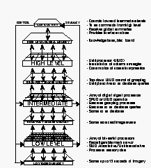
Figure 1. Overview of the IUA
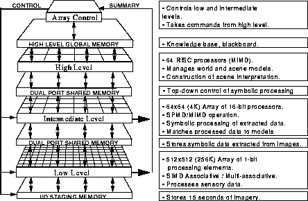
We begin by summarizing the characteristics of the first two generations of the IUA. Figure 1 is an overview of the IUA.
The first generation of the IUA3 is a proof-of-concept prototype containing 4K low-level (CAAPP) processors, 64 intermediate-level (ICAP) processors, and a single high-level (SPA) processor which also serves as the system host. The CAAPP processors are bit-serial, each with 320 bits of on-chip memory and 32K bits of backing-store memory. The ICAP processors are 16-bit TMS320C25 chips, each with 256K bytes of private memory, 256K bytes shared with 64 CAAPP processors, and 128K bytes shared with the SPA. The ICAP processors communicate via a centrally-controlled bit-serial crossbar switch, using their built-in serial communication channels. The SPA is any VME-bus compatible processor.
The Array Control Unit (ACU) for the prototype is a very simple memory buffer for streaming instructions to the array at a high rate. The ACU has no processing or branching capability, and thus all control flow is managed by the host. This arrangement is adequate for its purpose, testing and limited demonstrations of the system, but is not effective for real applications.
The CAAPP is a mesh-connected SIMD array with special I/O and communication features to support image understanding. In the first generation, each of the custom CAAPP processor chips contains 64 processors, and consists of roughly 160,000 transistors as shown in Figure 2. The chips were built in 2-micron CMOS technology via MOSIS.
Data is loaded into the CAAPP by writing to an image buffer, which is then shifted into all of the processor chips in parallel, via their nearest neighbor mesh. Output from the CAAPP follows the reverse of this process. In addition, the backing store memory of the CAAPP is dual- ported with the ICAP so that results from each CAAPP processor chip can be read by the corresponding ICAP processor chip via a direct data path. Thus, the aggregate transfer rate between the two levels scales with the size of the arrays.
Communication within the CAAPP is via both a standard mesh and a reconfigurable mesh that allows the array to be divided into independent groups of processors. Within each group, a single processor can be selected to broadcast a value, or a set of the processors can place bits on the network that are ORed with each other in a manner analogous to the global OR reduction circuit found in many SIMD arrays.
Figure 1. Overview of the IUA
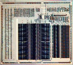
Figure 2. First Generation CAAPP Chip
The reconfigurable mesh is especially useful for supporting region- based processing in computer vision, where a region can be represented by an isolated group of processors corresponding to its constituent pixels in an image as illustrated in Figure 3.
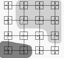
Figure 3. Isolated Processor Groups Corresponding to Regions in an Image
Because the processors in a group share common properties and purposes, we call the group a Coterie, and the network is known as the Coterie Network. The actual implementation permits signals to cross orthogonally or bypass a node diagonally. Thus, Coteries need not be physically adjacent to be linked.
The Coterie Network results in a new mode of parallelism that falls somewhere between SIMD and MIMD. While there is still a single instruction stream, broadcasting of data values and collection of summary information are no longer restricted to a central entity. We refer to this mode of parallelism as multiassociative.
In the first generation, I/O with the ICAP is performed by the SPA/host, via the dual-ported memory between the ICAP and the SPA/host, or via the CAAPP, if the data is in the form of an image. Physically, the IUA prototype consists of 16 12U circuit boards, plus additional boards for control, I/O and communication. The boards are sparsely populated for easy diagnosis and rework, as shown in Figure 4. The prototype system is shown in Figure 5.
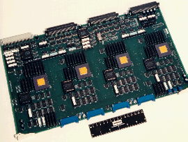
Figure 4. IUA First Generation Processor Board
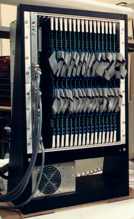
Figure 5. First Generation IUA Prototype
The second generation IUA retains the basic three-level structure of the prototype, but the SPA and host can be separate processors. For example, a commercially available multiprocessor could be used for the SPA, while the host can be any workstation on an ethernet. The new ACU is a full-fledged processor, consisting of a SPARC-based single- board computer and a microcode engine with a 128-bit instruction word and two separate arithmetic units (one for computation, and one for address arithmetic).
The full configuration for the second generation IUA contains 16K low-level processors, 64 intermediate-level processors, and four high- level processors. Physically, the processor array consists of only 8 12U processor boards each with memory daughter cards, plus additional boards for control and I/O.
Each of the processor cards contains 8 CAAPP chips and 8 ICAP chips as shown in Figure 6. These are divided into two quadnodes, each with four CAAPP-ICAP processor chip pairs.
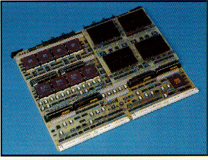
Figure 6. Second Generation Processor Board with One of Two Memory Daughter Boards Installed
At the CAAPP level, the basic bit-serial architecture is retained, but a 32-bit corner-turning register increases the on-chip memory to 352 bits per processor. The corner-turning register provides greater flexibility in formatting values that are to be passed to the ICAP. Image I/O with the CAAPP still involves writing to a frame buffer, but the data path to the buffer is now 128 bits wide, permitting a data rate of 160 MB per second. Once the data is in the frame buffer, it appears as merely another segment (HCSM) of backing-store memory (CISM) to the CAAPP processors. Thus, the time to load or store an image is the same as for any other backing store fetch. HCSM provides 4K bytes of storage for each CAAPP processor. CISM has further been doubled in size to 64K bits (8K bytes) per processor.
The CAAPP processor chip now contains 256 processors, and consists of roughly 600,000 transistors as shown in Figure 7. The chip is built in 1.2 micron CMOS and has been tested at its 10 MHz design speed.
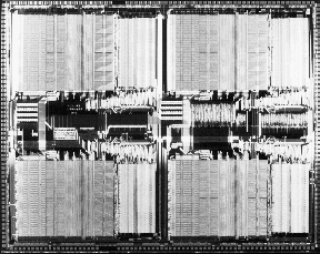
Figure 7: Second Generation CAAPP Chip
The ICAP level has been completely redesigned. It now uses the TMS320C40 32-bit processor, which contains both integer and floating-point units, and operates at up to 50 MFLOPS. Each ICAP processor has 1 MB of private storage in addition to the ability to access 2MB of memory that it shares with 256 CAAPP processors. ICAP processors are now arranged in groups of four to form a quadnode (see Figure 8). Each quadnode has a 4 MB local shared memory which is immediately accessible to the four processors.
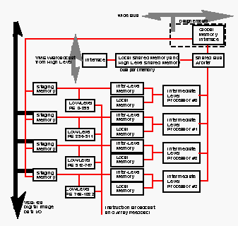
Figure 8. ICAP Bus Structure
Communication in the ICAP takes place via a set of message-passing channels. Each processor has six 8-bit channels together with six DMA controllers. Thus, each quadnode has a pool of 24 channels. Of these, 8 form a unidirectional token ring within the quadnode, 15 are bidirectionally connected to all of the other quadnodes, and the remaining channel is brought to an external connector for diagnostics, or custom I/O. In effect, each quadnode is directly connected to all other quadnodes via a 20 MB/S DMA channel, as shown in Figure 9. In addition, provision has been made in the system to support a 128-bit wide global bus that links the quadnode shared memories. The interface between the local shared memory bus and the global bus can be implemented with a daughter card that mounts on each processor card. Although the specification and a preliminary design for this daughter card were developed, its construction was not funded. The global bus interface is an optional part of the hardware that accelerates broadcasts and updating global variables, and provides redundancy in the communication system.
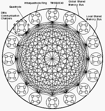
Figure 9. ICAP Communication Structure
The project was canceled at the start of 1995. The backplanes, chassis, and array control units for two systems had been constructed and tested. One of the memory daughter cards had also been built. The initial run of custom processor chips had been tested and found to be functional at full speed and a second production run of the chip had been prepared for fabrication of the required quantity of chips to populate the prototype systems. The remainder of the components required to populate the first two processor cards had been purchased. The printed circuit board layout for the processor cards had been finished.
The optimizing compiler for the parallel IUA C++ Class Library (ICL) had been tested on the ACU hardware, the ICAP support software had been completed up to the data transport level and development work had begun on the Intermediate-level Symbolic Representation (ISR) token database system1. The intermediate-level support software had been tested on a TMS320C40 multiple processor development board that was configured to resemble the TMS320C40 environment in the IUA.
Application software had been developed that demonstrated how the low- and intermediate-level software would work together. The application involved extracting a set of edgels with the software simulator for the low-level SIMD array, and transferring them to the intermediate-level MIMD hardware/software development platform where they would be symbolically grouped into straight lines. The results from the parallel implementation had been verified against the results obtained from a corresponding sequential algorithm.
The University of Massachusetts has mainly undertaken basic research efforts associated with the next generation IUA, focusing principally in three areas: the architectural performance analysis for future IUA hardware, development of advanced programming tools, and benchmark development. Hughes and Amerinex had been engaged in applied research, developing basic approaches to the next generation architecture, designing specific VLSI building blocks, exploring available technology options, and experimenting with the effects of interactions between compiler optimizations and processor architectures.
In preparation for the design of the next generation of the low-level processor in the IUA, we developed a performance evaluation system called ENPASSANT (ENvironment for PArallel System Simulation and ANalysis Tools). The system allows us to evaluate the performance of a wide range of features and parameters in a massively parallel array using execution traces of actual vision applications. ENPASSANT enables the user to evaluate the performance of SIMD arrays executing arbitrary programs written in the IUA C++ Class Library (ICL)5. The user can control such architectural features as the width of datapaths, memory hierarchy, communication network, components of the PE ALU, presence of floating point support, and so on. The system is also roughly two orders of magnitude faster than traditional trace-based simulations, In addition, its analysis is performed in a manner that compensates for mismatches between the algorithms and the architecture.
The speed of the system, and also the portability of code among the wide range of architectures that the user can specify, is due to the use of a virtual machine model (VMM) for massively parallel arrays (MPA). The VMM is based on the virtual model employed in ICL, extended with some additional parallel primitives such as Scan. The VMM high- level code is then executed directly by a virtual machine simulator that outputs a trace of its execution.
Once a trace is generated, it can be reused for evaluating many different architectural configurations, thus saving the time of regenerating the trace for every new configuration. Because the trace represents high- level operations (such as Route or Scan), it is also much more compact than traditional instruction-level traces.
In order to produce a detailed performance analysis, it is necessary to further process the trace to take into account the actual configuration of the target architecture. We call this processing trace compilation because it employs many of the same techniques as the back-end of a compiler, such as peephole optimization, register allocation, and register scheduling. The trace compiler also simulates the memory hierarchy in order to determine cache behavior for the trace. Finally, rather than generate actual code, however, the trace compiler looks up the execution cost for each operation from tables that are defined by the user as part of the architectural description, and then outputs performance in terms of basic clock cycles. Figure 10 shows a block diagram of the ENPASSANT system.
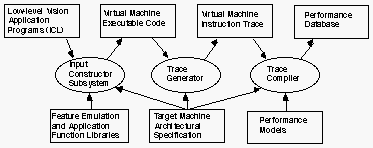
Figure 10. ENPASSANT System Overview
A mismatch can occur between algorithm and architecture when a parallel program is run on an machine that is significantly different from the one for which it was designed. This mismatch can lead to a significant loss of performance, even though it may be possible for the architecture to obtain better performance on the same task with a different algorithm. Because such a mismatch affects the fairness of comparing different architectures, an analysis system must deal with this problem. ENPASSANT allows the user to supply application function libraries with different algorithms for the same operation. The system then uses the appropriate algorithm, as indicated by the user, for each architectural configuration.
In addition, ENPASSANT provides a set of built-in emulations that enable any ICL program to be run on any configuration (albeit possibly with reduced efficiency). An example of such an emulation is the execution of a combining route operation on a machine that has only a nearest neighbor mesh (no dedicated router network).
We have already obtained interesting results from using ENPASSANT with a test suite of vision applications. For example, it has been found that a combination of a cache of about 500 bytes and a register file of about 50 bytes give better performance than configurations with just cache or register file, even when the cache or register file is significantly larger. We have also found that the smaller the cache line size the better, because there is little spatial locality to exploit in vision algorithms on MPAs (most of the usual spatial locality in sequential code comes from adjacent array references, but in an MPA the array is distributed and processed in parallel). It was also noted that a direct-mapped cache must be twice as large as an associative cache to achieve the same performance. Numerous other results are detailed in Herbordt's thesis.
After a survey of existing parallel languages we have determined that none support the greater heterogeneity that we expect to see in future vision systems. Some of the languages provide for one or a few models of parallel programming, but have no ability to adapt to new models or combinations of parallelism. Others provide extensibility, such as Ada or C++, essentially by allowing the user to build second-class types and constructs on top of the built-in ones.
For example, in Ada or C++, one can define a new matrix type with overloaded arithmetic operators so that it appears that matrix operations are being performed in parallel using arithmetic expressions. It is even possible to have these operations linked to library calls that execute on parallel hardware. However, the compiler is unable to apply traditional optimizations, such as common subexpression elimination, to this new type because it has no way of knowing that the matrix arithmetic function calls have the necessary algebraic properties.
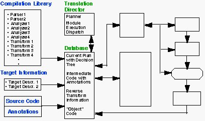
Figure 11. Compiler Framework for Heterogeneous Systems
We have thus begun to develop a new approach to compilation that is based on an open framework, as shown in Figure 11. The key elements of the framework are the compilation library, the translation director, and the database. Unlike traditional monolithic compilers that interweave the generation, processing, and deletion of intermediate information, the compilation framework retains all information generated during a compilation in a persistent object store. The processing of the user's code is performed by a series of independent modules that communicate via the object store. The execution of the modules is managed by the translation director.
For each compilation of a particular source to a particular target (or set of targets), the translation director assembles a customized plan for executing modules from the compilation library. The plan is based on a preliminary analysis of the code, annotations that have been attached to the code by the user, and the stored descriptions of the target machines. As further analyses reveal more information about the user's code, the translation plan may evolve in response.
We believe that this approach can support the programming of systems in which there are varying combinations of heterogeneous parallel and sequential processing resources. In many cases it will be possible to write parallel programs using the extensibility of existing languages together with user annotations, and yet generate highly optimized object code. The system will also be able to assist the user in managing the multiple algorithmic implementations of operations that are sometimes required to obtain the best performance from different parallel architectures. See also reference 6.
Benchmarks and test suites are an essential element of the architectural evaluation process. At the conclusion of the last ARPA workshop on vision benchmarks to test the performance of parallel architectures, it was recommended that the second IU Benchmark be extended with a second level task to add motion and tracking to the original task. We have now defined this new benchmark and developed a preliminary sample solution.
In order to reuse as much of the earlier benchmark as possible, the new benchmark operates on the same type of scenes -- a 2.5 dimensional mobile of rectangles with chaff, but in the new benchmark, the mobile and chaff are blown around the scene by an idealized wind to produce predictable motion. The motion involves movement of the entire mobile as a unit, and movement of its individual components. The motions are both translational and rotational, and they are controlled by reasonably realistic physical constraint models.
Unlike the previous benchmark, there are no fixed data sets. Given the number of frames that must be processed in a single test, it is too unwieldy to prepare the input data for distribution. Instead, we have developed a data set generator that can be used to repeatably produce the same image sequence from a set of input parameters. Users thus have the flexibility to generate data sets for digital storage, output to video media, or in real time by one machine for direct input to the machine under test.
The goal of the new benchmark is to test system performance over a long period of time so that, for example, caches and page tables will be filled and achieve steady-state behavior. The benchmark also explores I/O and real-time capabilities of the systems under test, and involves more high-level processing. Figure 12 shows a series of output frames from one test run of the benchmark, showing the kind of motion that the model and chaff can undergo. Every seventh frame in the sequence is shown in order to exaggerate the apparent motion. The highlighted rectangles are the mobile, and the others are the chaff. In the actual input images, the model and chaff rectangles are randomly assigned 8- bit gray levels, making them indistinguishable, except from their geometric relationships and motions.
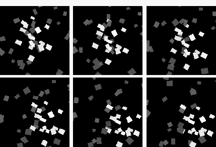
Figure 12. Sequence of Frames from Output of the ARPA IU Benchmark III
One of the issues that is driving the design of the next generation IUA is the reduction of cost and size in a system. This requires that the number of chips and circuit boards be greatly reduced. While VLSI device densities are increasing, this alone does not provide the desired reduction in package counts. Thus, a significant change in the architecture is required, at least for the low-level processor. In particular, it must be possible to build useful and viable systems that have just one or a small number of processor chips. Such a requirement implies that the processor chips must each process a larger portion of an image, or even that a single chip must be able to process an entire image. Because it is not yet possible to place as many processors on a chip as there are pixels in typical images, the implication is that virtual processors must be employed, and that the virtualization factor is quite large (e.g. mapping 512 or 1K virtual processors to each physical processor).
The original CAAPP architecture was designed to scale up to sizes that would reduce the virtualization factor to a small degree (i.e. less than 16). Transforming it into a design that can handle higher factors requires significant changes.
In addition, SIMD systems in general suffer from two problems that limit their speed: clock distribution and instruction dilation.
When a parallel array is virtualized, there are two general approaches one can take. Each processor can take responsibility for every Nth pixel in an image, where N is the number of processors, or for the M pixels in its immediate neighborhood, where M is the virtualization factor. The former case implies that neighboring processors always contain the neighboring pixels, and virtualization involves processing tiles of images in parallel and then handling the special processing at the edges of the tiles. In the latter case, each processor serially processes the pixels in a tile, emulating communication between virtual processors within itself, and communicating with adjacent physical processors when data must cross a tile boundary.
Our experience has shown that a combination of these virtualization methods must be employed in order to obtain the best performance. We plan to support a mode in which each chip is responsible for a 1/K contiguous portion of the image, where K is the number of chips in the system. Within a chip, each processing element operates on every Mth pixel in the part of the image assigned to the chip. The goal of supporting this mode of virtualization is to improve temporal locality in the on-chip caches and thereby reduce traffic to the main memory. Hardware virtualization support also permits the extensive use of prefetching techniques to hide memory latency. Even so, special high- bandwidth main memory, such as synchronous DRAM, is required to keep the processing elements from sitting idle.
Because the processing elements in a SIMD array operate synchronously, they must receive a globally generated clock signal. The clock signal must arrive at each processing element with a minimal amount of skew with respect to all others. Typically the skew must be less than 10% of the clock period in order for the processors to communicate. For example, in order to operate a SIMD array at 200 MHz, the clock skew should be kept to less than 500 picoseconds. However, it is very difficult to distribute a signal with low skew to thousands of processing elements because several levels of buffering are required to distribute the signal (each buffer introduces a slightly different delay) and because the processors themselves are at different physical distances from the clock generator. Typical variations are on the order of 5 to 10 nanoseconds for a large array. Hence, SIMD arrays have typically been limited to speeds of around 10 to 20 MHz. Thus, when building a system with just one or a few SIMD chips that is to be competitive with current serial machines (i.e. provide at least a factor of 100 higher performance) it is necessary to increase the clock rate of SIMD processors by roughly a factor of 10.
The approach that we will take to achieve this increase in clock rate is to abandon a purely synchronous regime and develop a SIMD processor that operates in a loosely synchronized manner. The processing elements will be designed to tolerate much higher clock skew in communicating with each other, while still operating at a high clock rate.
Another factor that limits the performance of SIMD systems is the time required to generate instructions for distribution to the processing elements. Each array instruction is produced by a series of operations in the ACU. For example, in a bit serial algorithm, the ACU must keep one or more bit-address indexes up to date, increment a loop counter, test for the termination condition, move the bit-addresses to the appropriate fields of the instruction, set some status bits, and transmit the instruction to the processors. If a typical RISC microprocessor is used as the ACU, it can take 20 to 50 ACU instructions to accomplish this for each array instruction. This factor represents a dilation of the number of array instructions to be issued and requires that the ACU execute instructions that many times faster than the array, in order to keep the array busy.
For an array that operates at 10 MIPS, it would be possible to use a processor that executes at 200 to 500 MIPS as a controller. However, if the clock rate of the array is to be increased by a factor of 10, then there is no hope of keeping it busy with a traditional microprocessor as a controller. Yet the cost of a custom controller is prohibitive, both in terms of the hardware and the software to drive it.
We will approach this problem by offloading some of the control functions from the central controller to the processing element chips. Each chip will be able to locally expand portions of a broadcast operation into a series of internal operations. Thus, the instruction issue rate for the controller can be reduced to a reasonable level, while keeping the array processing elements busy doing actual computation at a high clock rate. Figure 13 shows diagrammatically the components required to support high virtualization factors, high clock rates, and on- chip instruction expansion in addition to the traditional elements of a SIMD processing chip.
Figure 13. Block Diagram of A Next Generation IUA SIMD Array Processor Chip
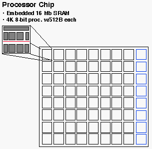
Figure 14. An Alternate Form of the Next Generation Low-Level Array
We are also exploring the design of an alternative low-level array architecture that would be useful in applications where performance outweighs flexibility and cost considerations. Rather than design a processor chip that handles high virtualization factors, the alternative architecture has no support for virtualization but is instead built with the same number of processors as there are pixels in an image. Each processing element has a limited amount of on-chip memory (e.g. 512 bytes) and no support for external memory. Using embedded ASIC SRAM, it will soon be possible to place as many as 4K processors on a single chip. These chips can then be assembled onto a multichip module (MCM) substrate to form an array with the appropriate number of processors for most medium-resolution sensors (i.e. on the order of 256K pixels).
For example, such an array could provide 256K 8-bit processors with a total of 128 MB of data memory. Operating at 80 MHz to keep power dissipation at reasonable levels, this array could still reach a peak performance of 20 trillion pixel operations per second. One of the major limitations of this approach is that once an array is built for a specific image format, it cannot be used for different formats. Thus, one of the research issues is to see if some additional flexibility for handing different image formats can be added without compromising the density of the design. Another area of research is to provide redundancy that enhances the MCM yield and fault tolerance in use.
Overall, the next generation IUA will retain its heterogeneous nature. It will have custom low-level processors, employ an off-the-shelf processor in a custom configuration for intermediate-level processing, and connect to a commercial uniprocessor or parallel system for high- level processing. However, the configuration of the system will no longer retain the fixed relationships and ratios between the processors at the different levels. It will be possible to assemble a wide variety of configurations in order to produce the most cost effective solutions for embedded applications.
For example, a system might be configured with multiple low-level arrays to simultaneously extract different features from imagery, and these could feed a single intermediate-level array, as shown in Figure 15. This flexibility of configuration is required in order to provide cost effective hardware for use in embedded applications. It is expected, however, that there will also be a standard workstation-compatible configuration for use by vision researchers and application developers.
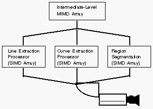
Figure 15. Possible System Configuration with Multiple Low-Level Arrays
The Image Understanding Architecture is undergoing significant change with the development of the next generation. Both the hardware and the software must be substantially enhanced. We expect the new system to be computationally more powerful than the earlier generations, and to be much more cost effective for embedded vision applications.
This work was funded in part by the Advanced Research Projects Agency (ARPA) under contract number DAAL02-91-K-0047, monitored by the U.S. Army Research Laboratory, contract numbers DACA76-86-C-0015, and DACA76-89-C-0016, monitored by the U.S. Army Engineer Topographic Laboratory; and contract number F49620- 86-C-0041, monitored by the Air Force Office of Scientific Research; and by an equipment grant (CDA-8922572) from the National Science Foundation (NSF).
Thanks also to David Schwartz, David Shu, Lap Chow, Dennis Finn, and Howard Neely at Hughes Research Laboratories for their contributions to the IUA design and development. At Amerinex Applied Imaging, Inc., Thomas Williams, James H. Burrill, Richard Lerner, Alfred Hough, Mike Freeman and Heidi Roskowski deserve credit for their extensive efforts in developing the IUA software. At the University of Massachusetts, the ENPASSANT system was developed by Martin Herbordt (now at the University of Houston) and the ARPA IU Motion Benchmark was developed by Glen Weaver and Steven Dropsho with assistance from Alan Boulanger in both efforts.
 burrill@cs.umass.edu